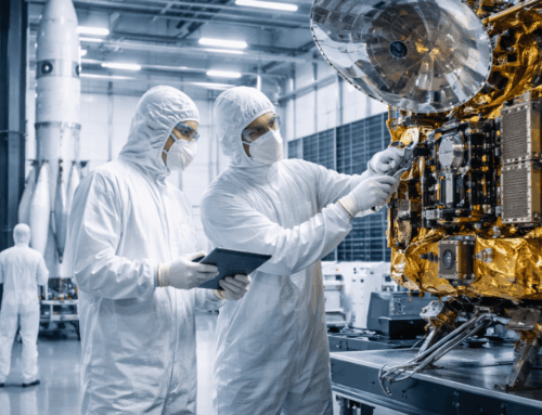
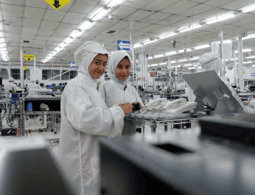
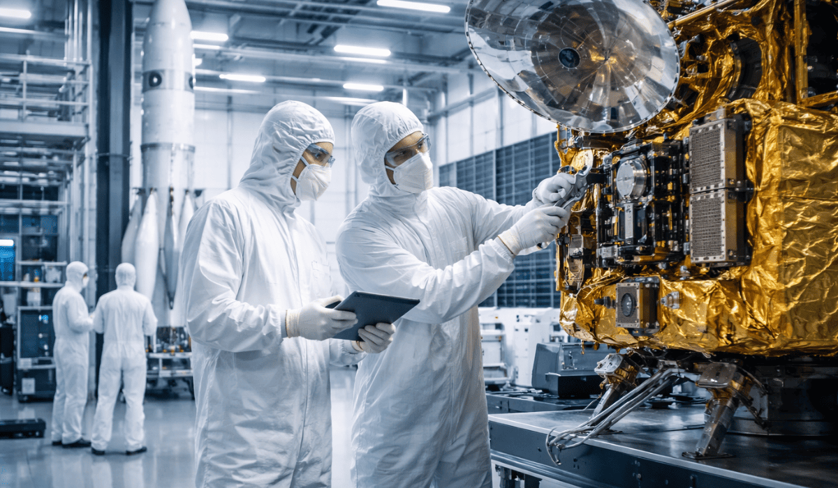
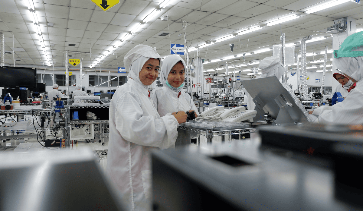
Semiconductor cleanrooms form the foundation of modern microchip manufacturing, where even microscopic contamination can disrupt yields, damage wafers, and compromise device performance.
As semiconductor geometries continue shrinking, cleanroom design, airflow control, filtration, and environmental stability become mission-critical engineering priorities rather than supporting infrastructure.
This guide outlines a practical roadmap for semiconductor manufacturing cleanrooms.
It covers design principles, contamination control strategies, airflow management, and advanced technologies required to maintain meticulous cleanroom environments.
What Makes Semiconductor Cleanrooms Uniquely Demanding
Semiconductor cleanrooms differ significantly from pharmaceutical or medical cleanrooms due to the extreme sensitivity of wafers, photoresists, and microelectronic components.
Key differentiators include:
- Sub-micron particle sensitivity
- Strict electrostatic discharge control
- Molecular and chemical contamination risks
- Continuous production cycles that demand stability
In semiconductor cleanroom construction, cleanliness does not operate as a single metric.
Particle contamination control, airflow behavior, and environmental precision must operate together as one integrated system.
Semiconductor Cleanroom Standards and Classifications
ISO Cleanroom Standards for Semiconductors
ISO cleanroom standards for semiconductors define allowable particle concentrations by size and volume.
Semiconductor fabrication facilities typically operate within ISO Class 1 through ISO Class 5 environments, depending on process sensitivity.
Advanced semiconductor nodes often require cleaner conditions than baseline ISO classifications suggest.
For this reason, semiconductor cleanroom requirements frequently exceed minimum ISO thresholds through process-specific controls.
Process-Driven Cleanliness Requirements
Semiconductor manufacturing cleanrooms rely on custom cleanliness targets tied directly to lithography accuracy, etching precision, and deposition quality.
Cleanroom environment control must align with equipment tolerances rather than generic classification labels.
Core Semiconductor Cleanroom Requirements
Particle Contamination Control
Particle contamination remains the primary threat inside semiconductor cleanrooms.
Common sources include personnel movement, tool vibration, material handling, and airflow disruption.
Effective semiconductor contamination control strategies include:
- High-efficiency filtration
- Controlled airflow patterns
- Zoning based on cleanliness sensitivity
- Reduced particle-generating materials
Even trace particle increases can translate into yield loss across production batches.
Airborne Molecular Contamination Control
Airborne molecular contamination control addresses gases, acids, bases, and organic compounds that settle invisibly on wafers.
These contaminants interfere with photolithography and chemical reactions.
Gas-phase filtration systems integrated into cleanroom HVAC systems for semiconductors help neutralize these threats before exposure occurs.
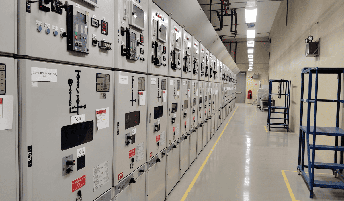
ESD Control in Cleanrooms
ESD control in cleanrooms protects sensitive semiconductor components from static discharge.
Flooring systems, grounded workstations, conductive garments, and humidity balance all contribute to effective static mitigation.
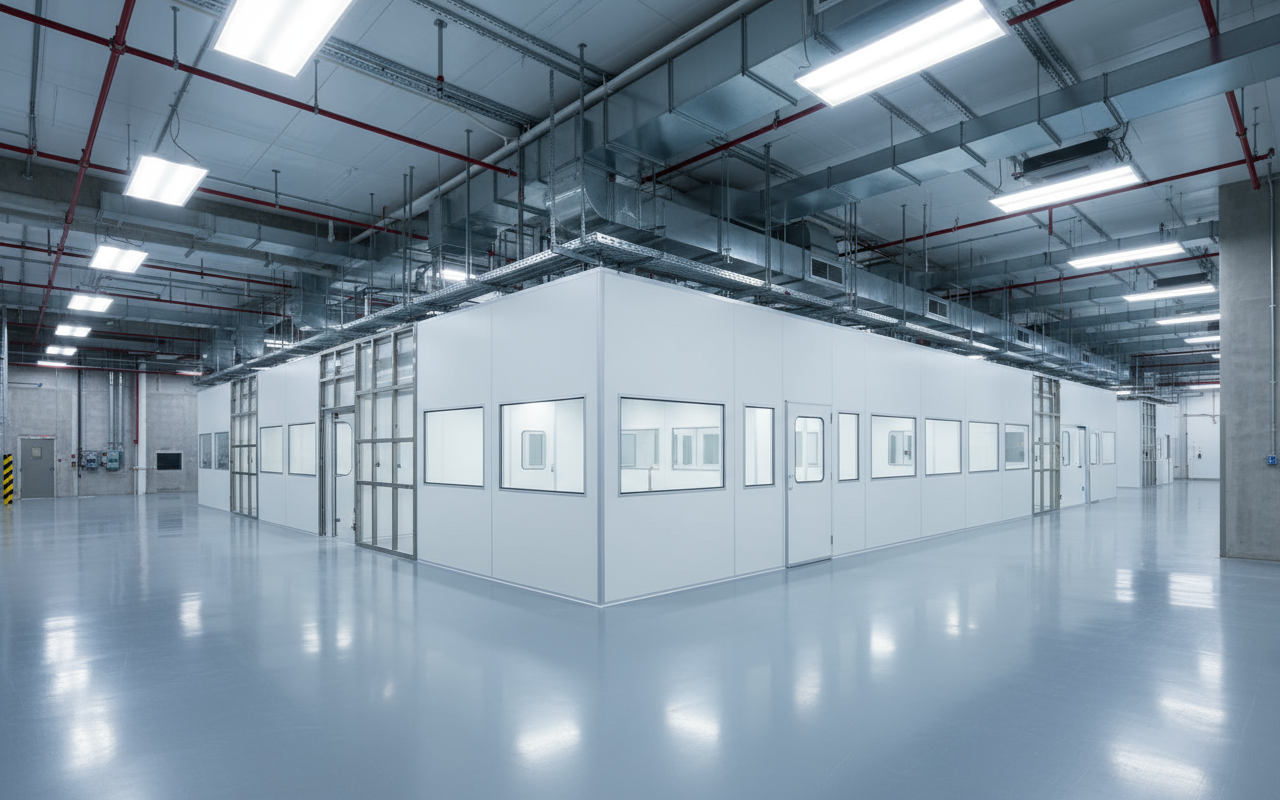
Semiconductor Cleanroom Design Fundamentals
Cleanroom Layout Planning
Semiconductor cleanroom layout planning prioritizes controlled movement of people, tools, and materials.
Zoning reduces cross-contamination risks and preserves pressure integrity across spaces.
Design considerations include:
- Personnel gowning sequences
- Equipment service corridors
- Material transfer pathways
- Segregated process zones
Semiconductor Cleanroom Construction Methods
Semiconductor cleanroom construction often relies on modular systems that support rapid deployment, scalability, and precise airflow integration.
Ceiling grids must support HEPA and ULPA filtration coverage without leakage or bypass.
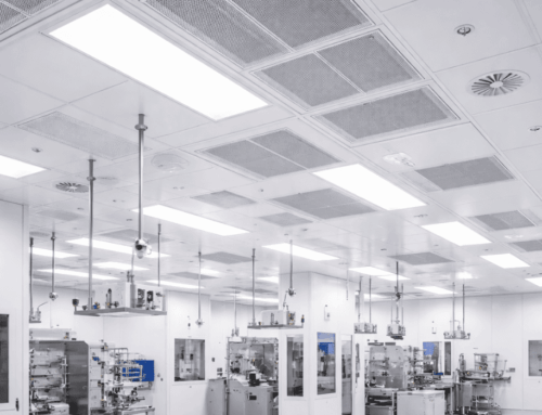
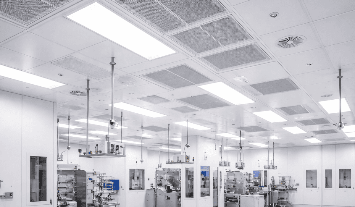
Airflow Management and Filtration Systems
Laminar Airflow Cleanroom Design
Laminar airflow cleanroom design directs filtered air in uniform streams across critical process areas.
Vertical laminar flow remains the dominant configuration in semiconductor manufacturing cleanrooms due to superior particle removal efficiency.
HEPA and ULPA Filtration
HEPA and ULPA filtration systems form the backbone of cleanroom airflow management.
ULPA filters capture particles down to 0.12 microns, making them essential for advanced semiconductor applications.
Proper filter placement, sealing, and maintenance protect airflow integrity over time.
Cleanroom Pressure Control
Cleanroom pressure control maintains positive pressure differentials between spaces.
This strategy prevents unfiltered air from entering sensitive zones and preserves cleanliness during door operation and personnel movement.
Environmental Control Inside Semiconductor Cleanrooms
Temperature Stability Requirements
Temperature fluctuations disrupt photolithography alignment and tool calibration.
Semiconductor cleanrooms demand tightly regulated thermal conditions with minimal variation across production cycles.
Redundant HVAC systems and continuous monitoring protect operational consistency.
Humidity Control in Cleanrooms
Humidity control cleanroom systems support both ESD mitigation and material stability.
Excess moisture introduces corrosion risks, and insufficient humidity increases static discharge potential.
Balanced humidity control protects wafers, tools, and personnel safety simultaneously.
Cleanroom Materials for Semiconductor Fabs
Cleanroom materials for semiconductor fabs must resist corrosion, shedding, and chemical exposure.
Surface finishes should support frequent cleaning without degradation.
Common material selections include:
- Non-porous wall panels
- Seamless conductive flooring
- Stainless steel or coated steel components
- Low-outgassing sealants
Each material choice directly impacts long-term contamination performance.
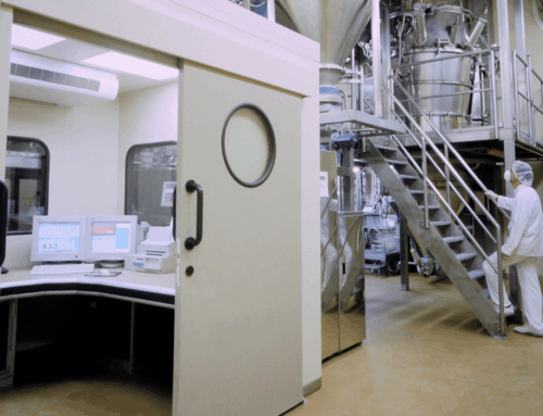
Applications of Semiconductor Cleanrooms
Semiconductor cleanrooms support a wide range of fabrication, research, and production activities across the microelectronics industry.
Primary applications include wafer fabrication, photolithography, etching, deposition, ion implantation, and advanced device packaging.
Research and development cleanrooms enable process innovation and prototyping under tightly controlled conditions.
High-volume production cleanrooms support repeatable manufacturing with stable yields and reduced defect rates.
As semiconductor technology advances, cleanrooms also support compound semiconductors, MEMS devices, power electronics, and advanced packaging technologies.
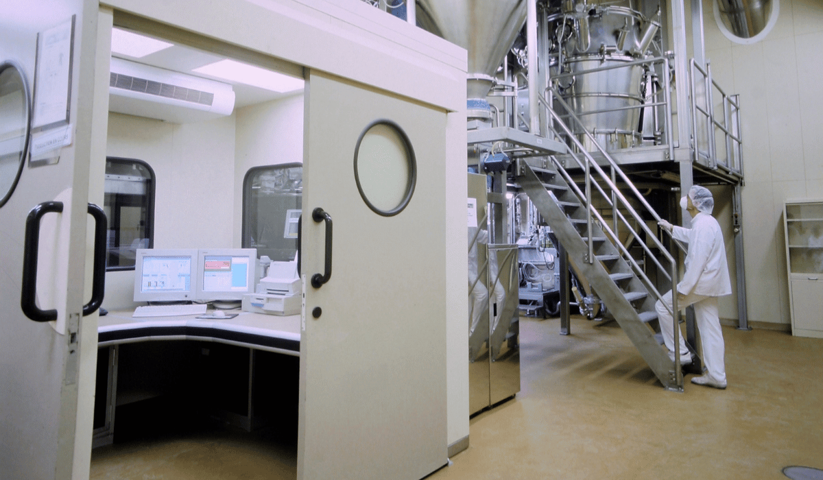
Monitoring and Continuous Control Systems
Cleanroom Monitoring Systems
Advanced cleanroom monitoring systems provide real-time data on particle levels, airflow velocity, temperature, humidity, and pressure.
These systems support rapid response before deviations affect production.
Certification and Performance Validation
Routine validation confirms compliance with semiconductor cleanroom requirements.
Certification testing evaluates airflow patterns, filter performance, and environmental stability across operating conditions.
Advanced Cleanroom Technologies for Semiconductor Manufacturing
Advanced cleanroom technologies play a critical role in supporting modern semiconductor manufacturing, where precision, repeatability, and operational efficiency must coexist.
As fabrication processes become more complex and device geometries continue to shrink, traditional cleanroom control methods are no longer sufficient on their own.
Technology-driven systems now form the backbone of high-performance semiconductor cleanrooms.
Automation is a central component of advanced cleanroom environments.
Automated airflow control systems dynamically regulate air volume, velocity, and distribution based on real-time cleanroom conditions.
These systems respond instantly to changes in particle levels, occupancy, and process activity, ensuring consistent contamination control across critical zones without manual intervention.
Predictive analytics further enhance cleanroom reliability by analyzing historical and real-time performance data from cleanroom monitoring systems.
Sensors tracking particle counts, pressure differentials, temperature, humidity, and filter performance feed data into analytics platforms that identify trends before deviations impact production.
This approach allows maintenance teams to address potential issues proactively, reducing unplanned downtime and protecting manufacturing yield.
Energy-efficient cleanroom HVAC systems for semiconductors represent another major advancement.
High-efficiency fan filter units, variable frequency drives, and optimized airflow strategies reduce energy consumption without sacrificing cleanliness.
Smart controls adjust airflow and filtration loads based on production demand, time of day, and process sensitivity, balancing operational cost with environmental precision.
Advanced filtration technologies also contribute to improved cleanroom performance.
Enhanced HEPA and ULPA filter designs deliver higher capture efficiency with lower pressure drop, improving airflow stability and reducing energy demand.
Gas-phase filtration systems target airborne molecular contamination, protecting wafers from chemical exposure that can interfere with lithography and deposition processes.
Integration between cleanroom systems and manufacturing equipment creates a unified control environment.
Cleanroom parameters can be synchronized with process tools, ensuring environmental conditions remain aligned with equipment requirements throughout each production stage.
This level of coordination supports consistent process outcomes and reduces variability across manufacturing cycles.
Together, these advanced cleanroom technologies transform semiconductor cleanrooms into intelligent, adaptive environments.
By combining automation, predictive analytics, energy-efficient infrastructure, and real-time monitoring, semiconductor manufacturers achieve higher reliability, improved yield protection, and scalable cleanroom performance aligned with future technology demands.
Conclusion
Semiconductor cleanrooms represent far more than controlled environments.
They serve as precision manufacturing platforms where airflow, filtration, materials, and monitoring converge to protect yield and innovation.
Investment in well-designed semiconductor cleanrooms delivers measurable returns through improved reliability, reduced defects, and scalable production capacity.
Partner With Cleanroom Experts for Semiconductor Precision
At UltraPure Technology, we help you build semiconductor cleanrooms designed for long-term performance.
Our cleanrooms are built for contamination control, airflow precision, and environmental stability.
Our team delivers cleanroom solutions aligned with advanced manufacturing demands, from concept through long-term operation.
Contact UltraPure Technology today to plan a semiconductor cleanroom engineered for precision, compliance, and performance.
Frequently Asked Questions
What are semiconductor cleanrooms?
Semiconductor cleanrooms are controlled environments designed to limit particles, chemical contaminants, and static electricity during chip manufacturing. These spaces protect wafers and microelectronic components from defects that impact yield, performance, and reliability.
Which ISO cleanroom class is used for semiconductor manufacturing?
Most semiconductor manufacturing cleanrooms operate between ISO Class 1 and ISO Class 5. Advanced lithography and wafer fabrication processes often require ISO Class 1 conditions to maintain extreme contamination control.
Why is contamination control critical in semiconductor cleanrooms?
Even microscopic particles can damage wafers and disrupt circuit patterns. Effective contamination control reduces defects, improves production yields, and supports consistent semiconductor manufacturing outcomes.
How does airflow management work in semiconductor cleanrooms?
Cleanroom airflow management relies on controlled laminar airflow that moves filtered air uniformly across critical zones. This airflow pattern removes particles efficiently and prevents contamination from settling on sensitive surfaces.
What filtration systems are used in semiconductor cleanrooms?
Semiconductor cleanrooms use HEPA and ULPA filtration to remove ultra-fine particles from the air. ULPA filters capture smaller contaminants, making them essential for advanced semiconductor processes.
Why is pressure control important in cleanroom environments?
Cleanroom pressure control maintains positive pressure between spaces to prevent unfiltered air from entering critical areas. Proper pressure differentials protect cleanliness during personnel movement and door operation.
How do temperature and humidity affect semiconductor cleanrooms?
Tight temperature and humidity control protect wafer stability, equipment accuracy, and electrostatic safety. Environmental fluctuations can disrupt manufacturing precision and increase defect risks.
What materials are best for semiconductor cleanroom construction?
Cleanroom materials for semiconductor fabs must resist corrosion, chemical exposure, and particle shedding. Non-porous panels, seamless flooring, and stainless steel components support long-term cleanliness.
How often should semiconductor cleanrooms be tested or certified?
Testing frequency depends on process sensitivity and operational requirements. Many semiconductor cleanrooms undergo routine certification to confirm airflow, filtration, and environmental performance remain within specifications.