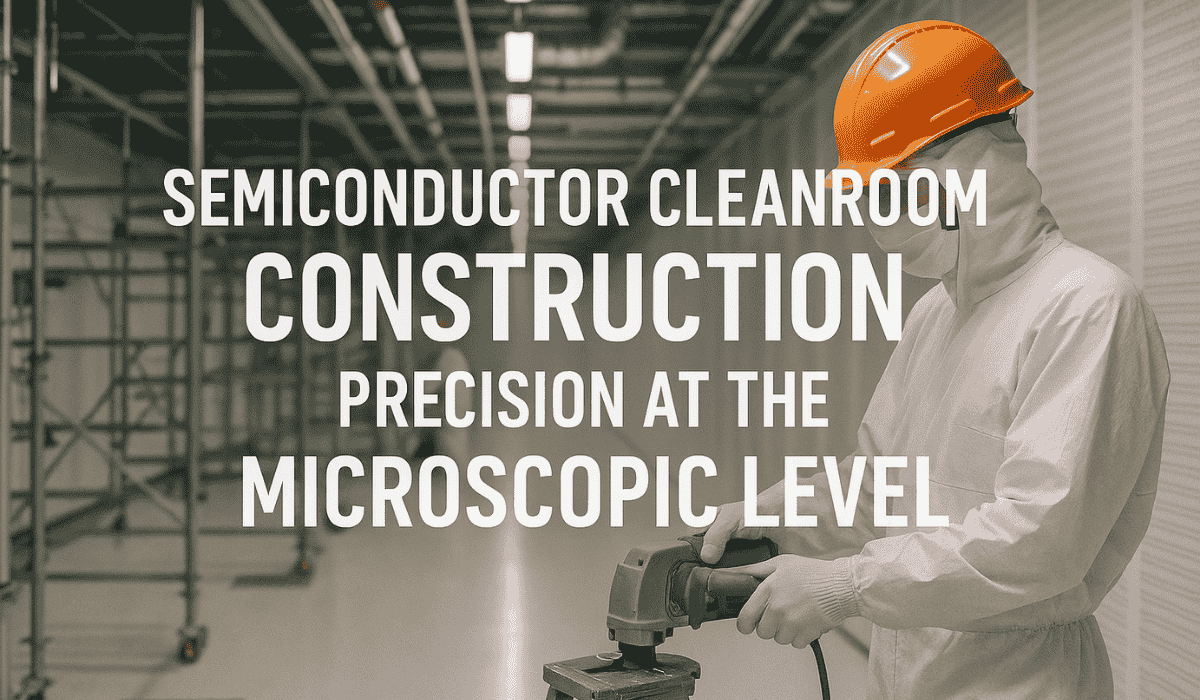
If there’s one place where precision truly defines success, it’s inside a semiconductor cleanroom.
In the world of microchips, one speck of dust, one vibration, or one degree of temperature fluctuation can ruin thousands of dollars’ worth of product. That’s why semiconductor cleanroom construction is one of the most demanding types of engineering in modern manufacturing.
At Ultrapure Technology, we’ve spent more than 30 years designing and building ultra-clean environments that power the future of technology — from semiconductor fabrication labs to microelectronics assembly.
In this article, we’ll explore what makes semiconductor cleanrooms so complex, how they differ from other cleanroom types, and why every detail — from airflow to flooring — matters at the microscopic level.
Why Semiconductor Manufacturing Needs Cleanrooms
Semiconductors are the brains of today’s technology. They’re used in everything — smartphones, cars, satellites, and even medical devices.
But manufacturing them requires absolute control over the environment.
Every transistor on a microchip is measured in nanometers — that’s one-billionth of a meter. At that scale, even a single airborne particle can short-circuit a wafer or destroy a microchip layer.
That’s why semiconductor cleanrooms exist: to maintain an environment free from dust, moisture, static electricity, and vibration so delicate manufacturing processes can happen flawlessly.
In short — cleanrooms make microchips possible.
The Standards That Define Semiconductor Cleanrooms
All cleanrooms are built to meet specific cleanliness levels defined by ISO 14644-1, which classifies rooms based on how many microscopic particles are allowed in each cubic meter of air.
Semiconductor fabrication typically takes place in ISO Class 5 or better environments.
To put that in perspective:
- ISO Class 5: Fewer than 3,520 particles per cubic meter (each smaller than half a micron).
- A typical office: Around 35,000,000 particles per cubic meter.
That’s nearly 10,000 times cleaner than everyday air.
Besides ISO 14644, semiconductor facilities must also comply with:
- IEST standards for airflow and filtration.
- SEMI S2 safety standards for equipment design.
- FM Global or NFPA guidelines for fire and material safety.
At Ultrapure Technology, our engineers design each cleanroom around these requirements to ensure full ISO, SEMI, and safety compliance.
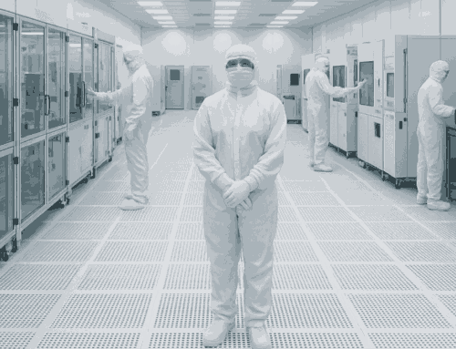
What Makes Semiconductor Cleanroom Construction Unique
Cleanrooms for semiconductor production are unlike any other controlled environments. They’re not just “clean” — they’re engineered ecosystems that balance air, pressure, temperature, and even electromagnetic fields with microscopic precision.
Here’s what makes them different:
1. Ultra-Clean Airflow and Filtration
Air cleanliness is the foundation of semiconductor manufacturing.
These cleanrooms use HEPA or ULPA filters that remove 99.999% of particles down to 0.12 microns.
Filtered air moves through the cleanroom in a laminar flow — a smooth, uniform stream that constantly pushes particles down and away from wafers and tools.
Ceilings are often 80–100% filter coverage, with air entering from above and exiting through perforated raised floors. This continuous flow keeps every square inch of air in motion, ensuring contaminants are immediately flushed out.
2. Precise Temperature and Humidity Control
Semiconductor materials are extremely sensitive to thermal changes. A difference of just ±0.1°C can affect layer alignment during lithography.
That’s why these cleanrooms maintain:
- Temperature: ±0.1 °C
- Humidity: 40–50% relative humidity
Automated HVAC systems adjust air conditions thousands of times per day to keep the environment stable.
This level of precision prevents static buildup and keeps photoresist coatings consistent across wafers.
3. Static and ESD Protection
Electrostatic discharge (ESD) is another major threat. A spark invisible to the eye can instantly destroy microchips.
Semiconductor cleanroom construction includes:
- Conductive flooring systems that dissipate static safely.
- Grounded benches, tools, and equipment.
- ESD-safe garments for every worker.
Even humidity control is part of ESD protection — dry air increases static risk, so maintaining proper moisture levels is essential.
4. Vibration and Noise Isolation
Microchip fabrication uses highly sensitive optical equipment, such as photolithography scanners and etching tools, that rely on perfect alignment.
Even tiny vibrations from nearby machinery or foot traffic can blur microscopic patterns.
To prevent this, semiconductor cleanrooms are built with:
- Floating slab floors or vibration-dampening mounts.
- Isolated structural supports for heavy equipment.
- Noise-controlled HVAC systems to avoid acoustic interference.
Every square foot is engineered to eliminate disturbance — even the hum of a nearby motor can impact yield.
5. Zoned Air Pressure Design
Semiconductor cleanrooms use a pressure cascade system to keep contaminants from migrating into critical zones.
High-pressure air flows from the cleanest areas (like wafer processing) to less critical support zones. This constant outward airflow ensures unfiltered air never enters sensitive spaces.
6. Material and Surface Selection
All materials used in semiconductor cleanrooms must be non-shedding, non-porous, and chemically stable.
Common materials include:
- Powder-coated aluminum wall systems.
- Stainless steel framing and supports.
- Anti-static epoxy or vinyl flooring.
- Smooth, seamless ceiling tiles and wall joints.
These surfaces are easy to clean, won’t generate dust, and resist corrosion from chemical vapors used in production.
7. Modular Flexibility for Rapid Expansion
The semiconductor industry evolves fast. New chip designs, new equipment, and new materials appear every year.
That’s why many manufacturers choose modular cleanroom systems that can be expanded or reconfigured quickly.
Ultrapure Technology offers modular and hybrid construction options, allowing facilities to upgrade ISO classes, add new zones, or relocate without full reconstruction.
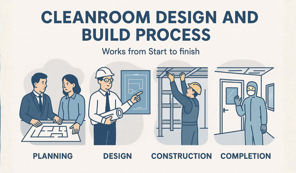
The Cleanroom Construction Process for Semiconductors
Building a semiconductor cleanroom follows a carefully planned sequence to guarantee precision and compliance.
Step 1 – Consultation and Design
Every project begins with a deep understanding of your manufacturing process — wafer size, equipment type, and required ISO class.
Our design team creates 3D models and airflow simulations to predict performance before construction begins.
Step 2 – Engineering and Material Selection
We design HVAC, filtration, electrical, and grounding systems customized for your process needs.
All materials are selected for low outgassing, static resistance, and durability in high-purity environments.
Step 3 – Construction and Installation
Modular wall systems, raised floors, and ceiling grids are installed with precision alignment.
Airflow and HVAC components are integrated to meet ISO 5 or stricter requirements.
Electrical and gas lines are grounded and sealed to maintain pressure integrity.
Step 4 – Testing and Validation
Once construction is complete, Ultrapure performs a full suite of tests:
- Airflow velocity and uniformity checks
- Particle count verification
- Pressure differential and leak testing
- Temperature and humidity mapping
- ESD and vibration validation
Only after every test passes do we deliver your cleanroom for production.
Benefits of Partnering with Ultrapure Technology
When it comes to building advanced cleanrooms, experience matters.
Ultrapure Technology brings over three decades of expertise to every project, combining innovation with proven results.
Our clients choose us because we provide:
- Turnkey design-build services — one team for design, engineering, and construction.
- ISO, SEMI, and ESD-compliant systems ready for validation.
- Faster project timelines using modular cleanroom components.
- Scalable solutions that adapt to future technologies.
- Nationwide experience with over 500 cleanroom installations.
Whether you’re expanding a fab facility or developing a new R&D lab, we deliver precision environments built for the next generation of technology.
Final Thoughts
Building a semiconductor cleanroom isn’t just about meeting ISO standards — it’s about creating a perfectly balanced environment where precision manufacturing can happen at the atomic level.
From air pressure to humidity to vibration control, every decision in construction impacts product quality and yield.
At Ultrapure Technology, we design and build cleanrooms that go beyond compliance — we deliver performance, reliability, and confidence.
If your company is preparing to expand semiconductor or microelectronics production, our team can help you create a cleanroom that’s certified, efficient, and ready for tomorrow’s technology.
Contact Ultrapure Technology today to start your semiconductor cleanroom project.
Frequently Asked Questions (FAQs)
What is a semiconductor cleanroom and why is it important?
A semiconductor cleanroom is a controlled environment designed to remove dust, static, and other contaminants that can damage microchips during manufacturing. It maintains precise temperature, humidity, and airflow conditions to protect delicate wafers and circuits. Even the smallest airborne particle can ruin a chip, which is why cleanrooms are essential for consistent quality and yield in semiconductor production.
What ISO class is required for semiconductor manufacturing?
Most semiconductor fabrication areas require ISO Class 5 or better, as defined by the ISO 14644 standard. This means fewer than 3,520 particles per cubic meter of air — far cleaner than typical pharmaceutical or medical cleanrooms. Supporting zones, like packaging or inspection rooms, may use ISO Class 6 or 7, depending on sensitivity. The cleaner the air, the higher the yield and reliability of the chips produced.
How does cleanroom design prevent contamination in semiconductor production?
Semiconductor cleanrooms use laminar airflow systems, where filtered air moves in a single direction from ceiling to floor to sweep out particles. HEPA or ULPA filters remove contaminants as small as 0.12 microns, while positive air pressure keeps dirty air out. Every surface is non-shedding, and workers wear full protective gear to prevent dust or static from entering critical areas.
Why is vibration control so critical in semiconductor cleanroom construction?
Manufacturing processes like lithography and etching use equipment that aligns patterns on wafers at the nanometer scale. Even the slightest vibration — from nearby machines or footsteps — can blur or misalign these patterns. That’s why semiconductor cleanrooms use vibration-dampening floors, isolated foundations, and quiet HVAC systems to maintain absolute stability during production.
How does Ultrapure Technology ensure compliance in semiconductor cleanroom projects?
Ultrapure Technology follows ISO 14644, SEMI, and ESD safety standards for every cleanroom design. Our in-house engineers handle design, construction, and validation to ensure full regulatory compliance. We test airflow, particle counts, humidity, vibration, and pressure before certification. Each cleanroom we deliver is turnkey, audit-ready, and optimized for long-term performance and precision manufacturing.
